What is a bill of materials’ role in PCB design?
Before building any new product, you need to know that you have the right materials available. Think of it like baking: if you don’t have any flour, you’re not going to end up with much of a cake.
A list of exactly what parts you need — and in what quantity — is essential to manufacturing, engineering, and parts design. When you have this information upfront, you expedite the procurement process. Thankfully, the bill of materials (BOM) provides exactly that. This is especially true for printed circuit boards (PCBs) and printed circuit board assemblies (PCBAs).
Below, we’ll highlight the importance of a thorough BOM when designing PCBs and the benefits of splitting your PCB BOM into two parts.
Duro’s cloud-native Product Lifecycle Management platform enables you to create a structured eBOM and publish all related engineering documents. Schedule a demo to learn more.
What is a bill of materials (BOM) in PCB design?
A bill of materials (BOM) is a comprehensive list of all the components needed to build a product. It includes part names, descriptions, and specs so that when it’s sent to the procurement team, they understand exactly what they need to source. Depending on the product’s size and complexity, its BOM could list just a few parts or hundreds.
In PCB design, there are two separate elements: the PCB and the PCB assembly (PCBA). Unlike traditional mechanical assembly, where you can have multiple nested levels, a circuit board only has a bottom level (the PCB itself) and top level (the PCBA with all attached components).
With a few rare exceptions, all electrical devices are built using a printed circuit board assembly. In an electro-mechanical product, the electrical components need to be mounted to something. All of the components have to be present, connected, and wired together in order for the device to work — and a PCBA is the most effective way to do that.
Without a complete and accurate BOM, the PCBA could have missing or wrong parts, resulting in a non-functional device that needs to be scrapped or sent for rework.
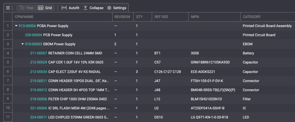 Example of a PCBA in Duro showing the top level PCBA itself with the the PCB and EBOM nested below.
Fields required in a BOM for PCB design
In PCB manufacturing, you’ll need to include a few required fields to build a complete and thorough BOM:
1) Item name
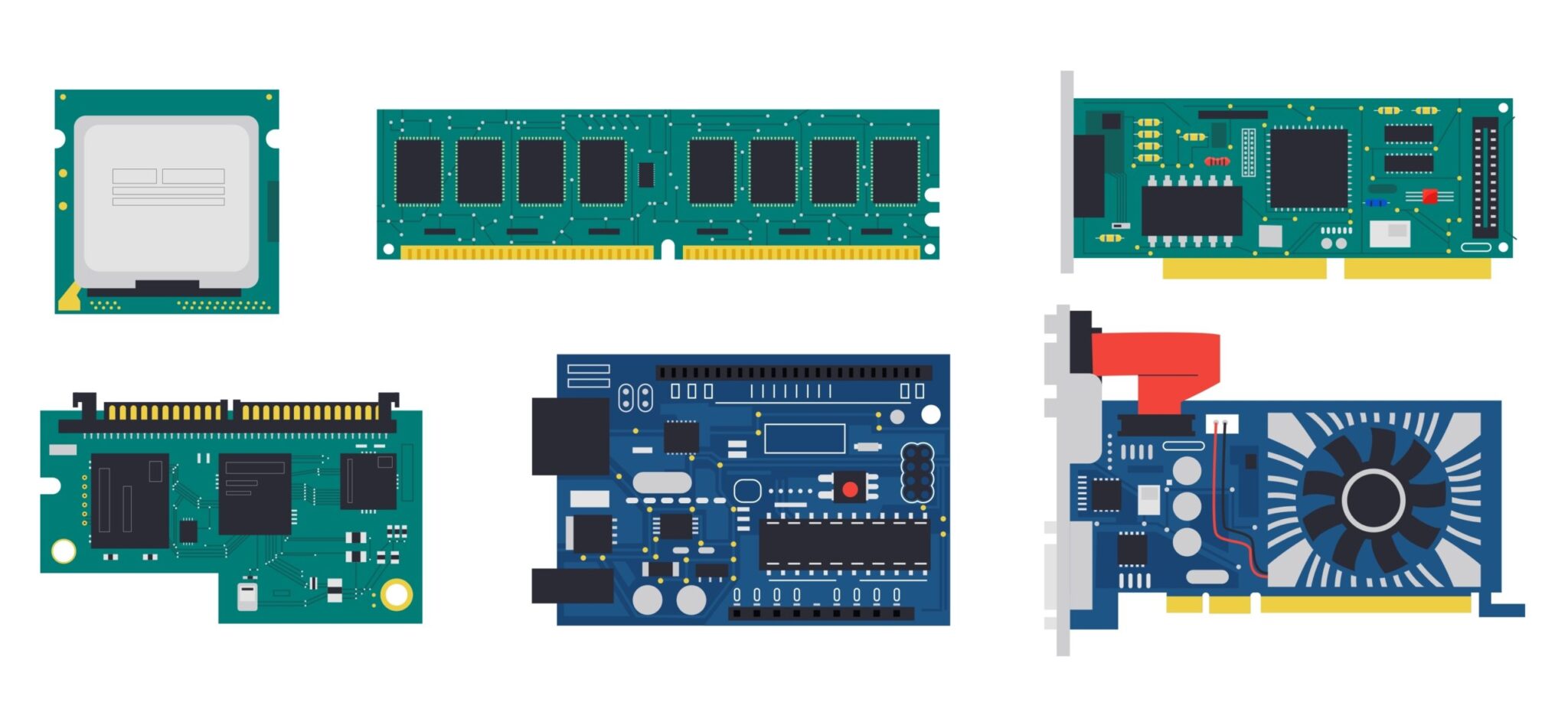
The first field that needs to be included in your BOM is the item name. This is where you’ll include both the printed circuit board and each of its attached individual components. Examples of these components include:
- Circuit board
- Capacitors
- Passers
- Resistors
- Diodes
- Connectors
2) Quantity per board
The quantity per board is a specification in the BOM that indicates the quantity of each part needed to create a single board assembly.
3) Manufacturer Part Number
The Manufacturer Part number (MPN) is a unique, specific identifier given to individual parts, typically appearing as a string of numbers and letters. This number tells your procurement team and vendors exactly which parts you need and is what you’d use to track materials through the manufacturing process.
It’s important to note that the MPN is a unique, internationally-used number and is not the same as the stock-keeping unit (or SKU), which is a vendor-assigned identifier for internal use and not relevant to board production.
4) Do not populate/Do not install (DNP/DNI)
This field indicates that a certain component is not needed for a particular version of the product.
5) Reference designator of components
A reference designator is an identifier used in the BOM to help identify where each component is referenced in the electrical schematic. The reference designator helps to eliminate any confusion regarding the location of each part on a board.
6) Size/footprint
Each component in a PCB will have different dimensions and layouts. This field often includes a diagram that shows where the components are located, including pins and leads. This information ensures that each component is placed correctly and that all components fit within their designated space.
7) Part description
The description of the part is how you add further information and details about each part to the BOM. You can use this field to describe the part’s function, add information about where to find the part, or suggest alternative parts to use if the Procurement team can’t source the original component.
Optional items
In addition to these mandatory items on a PCB BOM, there are a few other optional fields that can be used to further detail the comprehensive list of materials needed to create a printed circuit board assembly.
- Vendor name: The vendor’s name can help determine where the parts are being sourced from and who is distributing them to you.
- Vendor part number: Vendors might have their own part numbers for materials, so you may want to include that in your BOM.
- Value of the particular part: The value of the part indicates to teams the value associated with it and how it fits into the PCB.
- Part manufacturer name: This identifies where the part is produced and where you’ll get it from.
PCB schematics and documents
A PCB schematic is an internal pictorial representation of the final product that will be assembled. Rather than being a direct diagram of parts, the schematic is more of a functional representation of what the circuit board will look like.
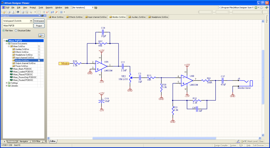 Example of a PCB schematic in Altium CAD.
Beyond the BOM, there are a few other critical documents related to PCB assembly:
- GERBER files: A collection of unique files that describe how to fabricate the printed circuit board and, in some cases, how to place the parts.
- Manufacturing document: A manufacturing document defines how the printed circuit board is fabricated, including materials, the specifics of the copper, and specifics of any kind of tolerances.
- Board file: Lays out exactly how components will be placed on the final board.
- Functional diagrams for components: Each component part can have its own detailed diagram outlining its specs, functions, and connections.
What are the different types of PCBs?
Not all PCBs are created equal; they can come in a variety of different layouts and serve different purposes. Here are a few of the most common PCB types and their applications.
Single side PCB
A single side PCB contains a single conductive layer placed above the substrate where electronic components are soldered or placed onto one side. Because they have only one conductive layer, the paths can’t overlap or take up too much space. These are great for low-density product designs like calculators and lighting boards and tend to be both cost-effective and easy to manufacture.
Double sided PCB
A double sided PCB, as the name might suggest, has conductive material on both the bottom and top of the substrate board. This allows the parts to be placed on both sides and connected through holes in the board. These types of boards are used for products that need smaller circuit boards than a single side PCB will allow, such as cell phones. Double sided PCBs increase the flexibility of the board and make it suitable for automotive dashboards, power amplifiers, and industrial controls.
Multi-layer PCB
A multi-layer PCB will have more than two conductive layers. The substrate and conductive layers are arranged in a “sandwich” layout that stack on top of each other. These different layers must then be laminated to avoid air gaps and ensure that components connect. These are used for advanced electronic products like heart monitors, x-ray machines, satellite systems, space probe equipment, and weather analysis. They are even more compact and offer a high level of design flexibility.
Rigid PCB
A rigid PCB has a firm circuit board that cannot be manipulated. It gives added strength to the board and is composed of multiple layers tightly adhered together. These boards are both compact and lightweight but cannot be modified once made. Rigid PCBs are often used in robotics and automotive production, and due to their ability to withstand vibrations and extreme temperatures, they are also used in aerospace and large, complex medical technology (MR systems and EKG machines).
Flex PCB
A flex PCB is the opposite of a rigid PCB. This flexible board is made out of movable materials like polyamide. The board is designed to move and bend without destroying the components attached to the board. It’s used for products like flex solar cells, cameras, and some automotive devices. They can save space in a design and help provide thermal management for products.
Rigid flex PCB
A rigid flex PCB is a hybrid board that is made of both flex and rigid components. This creates an end product that can both be folded and manipulated while still maintaining a high level of strength. Their flexibility and strength make them more complicated to create, but ideal for medical applications like cochlear implants and pacemakers, and aerospace technology like radar equipment and radio communications systems.
Why you should split your PCBA BOM into two parts: PCB and eBOM
At Duro, we recommend splitting your PCBA BOM into two different parts: the PCB itself and the eBOM, or electrical bill of materials for all the component parts. In addition to simplifying the process from your computer-aided design (CAD) software, there are some other key reasons why we consider this a best practice:
Simplifies independent revisioning
When your PCB and its components are laid out on two separate levels, it becomes much easier to make revisions to each level independently. For example, you might decide that a chip in your board is too close to where a mechanical enclosure comes together and decide to nudge the chip a millimeter to the left. In this instance, you would only need to revise the PCB itself — not the entire eBOM — because you’re only adjusting the location of one of the components.
Sometimes the assembly house and the fab house are not the same
Having a separate PCB and eBOM also makes it simpler to communicate information. For example, you might send the entire PCB assembly structure to one vendor to have it fabricated for you. However, they might split it up because it’s not always the case that the assembly house is also the fabrication house. If the PCB and eBOM are already separate, you can easily separate information and send it to the right party.
How PLM helps centralize your PCB and eBOM
Businesses often face challenges centralizing PCB and eBOM data. Transferring the information from CAD into an Excel spreadsheet and then into a product lifecycle management (PLM) tool can be time consuming. The tools aren’t set up the same way and it can involve renaming and creating new columns. This can lead to confusion, input errors, and miscommunication between teams.
However, Duro PLM can recognize columns from an Excel sheet and understand their context in the eBOM. Additionally, Duro has the ability to integrate with ECAD tools (like Altium), allowing you to transfer BOM information directly from your CAD tool. This skips the step of manually transferring data and results in fewer errors as all part information is centralized in the PLM system.
Using a PLM like Duro can automate this process, greatly reducing manual data entry and leading to cleaner, more accurate (and complete) eBOMs.
Manage your bill of materials and bring products to life faster with Duro
Duro PLM is a powerful tool that helps you manage your bill of materials with ease and store all the documents you need in one single source of truth. You can easily share materials across your organization and avoid the issues that add time to a product launch.
To learn more about Duro, schedule a demo and see for yourself how your business can be transformed with our help.